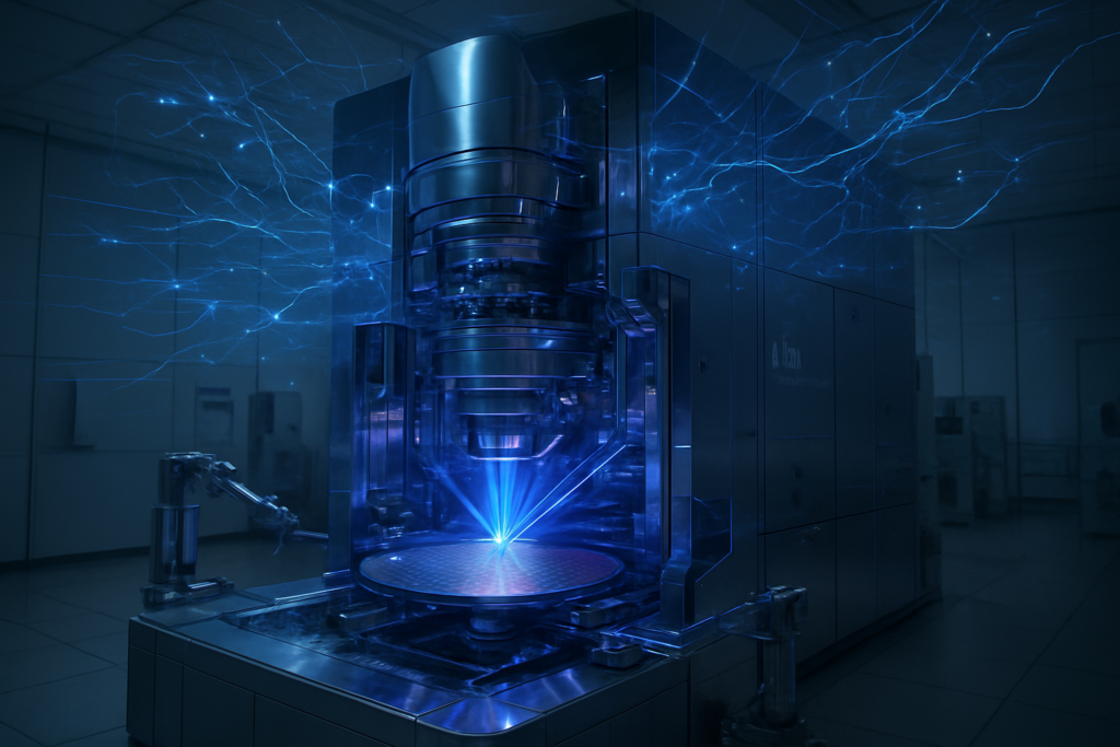
In a move that signals a tectonic shift in the global semiconductor landscape, Intel (NASDAQ: INTC) has officially entered the "High-NA" era. As of late December 2025, the company has successfully completed the installation and acceptance testing of the industry’s first commercial-grade High-NA (Numerical Aperture) Extreme Ultraviolet (EUV) lithography system, the ASML (NASDAQ: ASML) Twinscan EXE:5200B. This $350 million marvel of engineering, now operational at Intel’s D1X research facility in Oregon, represents the cornerstone of Intel's ambitious strategy to leapfrog its competitors and regain undisputed leadership in chip manufacturing by the end of the decade.
The successful operationalization of the EXE:5200B is more than just a logistical milestone; it is the starting gun for the 1.4nm (14A) process node. By becoming the first chipmaker to integrate High-NA EUV into its production pipeline, Intel is betting that this massive capital expenditure will simplify manufacturing for the most complex AI and high-performance computing (HPC) chips. This development places Intel at the vanguard of the next generation of Moore’s Law, providing a clear path to the 14A node and beyond, while its primary rivals remain more cautious in their adoption of the technology.
Breaking the 8nm Barrier: The Technical Mastery of the EXE:5200B
The ASML Twinscan EXE:5200B is a radical departure from the "Low-NA" (0.33 NA) EUV systems that have been the industry standard for the last several years. By increasing the Numerical Aperture from 0.33 to 0.55, the EXE:5200B allows for a significantly finer focus of the EUV light. This enables the machine to print features as small as 8nm, a massive improvement over the 13.5nm limit of previous systems. For Intel, this means the ability to "single-pattern" critical layers of a chip that previously required multiple, complex exposures on older machines. This reduction in process steps not only improves yields but also drastically shortens the manufacturing cycle time for advanced logic.
Beyond resolution, the EXE:5200B introduces unprecedented precision. The system achieves an overlay accuracy of just 0.7 nanometers—essential for aligning the dozens of microscopic layers that constitute a modern processor. Intel has also been working closely with ASML to tune the machine’s throughput. While the standard output is rated at 175 wafers per hour (WPH), recent reports from the Oregon facility suggest Intel is pushing the system toward 200 WPH. This productivity boost is critical for making the $350 million-plus investment cost-effective for high-volume manufacturing (HVM).
Industry experts and the semiconductor research community have reacted with a mix of awe and scrutiny. The successful "first light" and subsequent acceptance testing confirm that High-NA EUV is no longer an experimental curiosity but a viable production tool. However, the technical challenges remain immense; the machine requires a vastly more powerful light source and specialized resists to maintain speed at such high resolutions. Intel’s ability to stabilize these variables ahead of its peers is being viewed as a significant engineering win for the company’s "five nodes in four years" roadmap.
A Strategic Leapfrog: Impact on the Foundry Landscape
The immediate beneficiaries of this development are the customers of Intel Foundry. By securing the first batch of High-NA machines, Intel is positioning its 14A node as the premier destination for next-generation AI accelerators. Major players like NVIDIA (NASDAQ: NVDA) and Microsoft (NASDAQ: MSFT) are reportedly already evaluating the 14A Process Design Kit (PDK) 0.5, which Intel released earlier this quarter. The promise of higher transistor density and the integration of "PowerDirect"—Intel’s second-generation backside power delivery system—offers a compelling performance-per-watt advantage that is crucial for the power-hungry data centers of 2026 and 2027.
The competitive implications for TSMC (NYSE: TSM) and Samsung (KRX: 005930) are profound. While TSMC remains the market share leader, it has taken a more conservative "wait-and-see" approach to High-NA, opting instead to extend the life of Low-NA tools through advanced multi-patterning for its upcoming A14 node. TSMC does not expect to move to High-NA for volume production until 2028 or later. Samsung, meanwhile, has faced yield hurdles with its 2nm Gate-All-Around (GAA) process, leading it to delay its own 1.4nm plans until 2029. Intel’s early adoption gives it a potential two-year window where it could offer the most advanced lithography in the world.
This "leapfrog" strategy is designed to disrupt the existing foundry hierarchy. If Intel can prove that High-NA EUV leads to more reliable, higher-performing chips at the 1.4nm level, it may lure away high-margin business that has traditionally been the exclusive domain of TSMC. For AI startups and tech giants alike, the availability of 1.4nm capacity by 2027 could be the deciding factor in who wins the next phase of the AI hardware race.
Moore’s Law and the Geopolitical Stakes of Lithography
The broader significance of the High-NA era extends into the very survival of Moore’s Law. For years, skeptics have predicted the end of transistor scaling due to the physical limits of light and the astronomical costs of fab equipment. The arrival of the EXE:5200B at Intel provides a tangible rebuttal to those claims, demonstrating that while scaling is becoming more expensive, it is not yet impossible. This milestone ensures that the roadmap for AI performance—which is tethered to the density of transistors on a die—remains on an upward trajectory.
However, this advancement also highlights the growing divide in the semiconductor industry. The $350 million price tag per machine, combined with the billions required to build a compatible "Mega-Fab," means that only a handful of companies—and nations—can afford to compete at the leading edge. This creates a concentration of technological power that has significant geopolitical implications. As the United States seeks to bolster its domestic chip manufacturing through the CHIPS Act, Intel’s High-NA success is being touted as a vital win for national economic security.
There are also potential concerns regarding the environmental impact of these massive machines. High-NA EUV systems are notoriously power-hungry, requiring specialized cooling and massive amounts of electricity to generate the plasma needed for EUV light. As Intel scales this technology, it will face increasing pressure to balance its manufacturing goals with its corporate sustainability targets. The industry will be watching closely to see if the efficiency gains at the chip level can offset the massive energy footprint of the manufacturing process itself.
The Road to 14A and 10A: What Lies Ahead
Looking forward, the roadmap for Intel is clear but fraught with execution risk. The company plans to begin "risk production" on the 14A node in late 2026, with high-volume manufacturing targeted for 2027. Between now and then, Intel must transition the learnings from its Oregon R&D site to its massive production sites in Ohio and Ireland. The success of the 14A node will depend on how quickly Intel can move from "first light" on a single machine to a fleet of EXE:5200B systems running 24/7.
Beyond 14A, Intel is already eyeing the 10A (1nm) node, which is expected to debut toward the end of the decade. Experts predict that 10A will require even further refinements to High-NA technology, possibly involving "Hyper-NA" systems that ASML is currently conceptualizing. In the near term, the industry is watching for the first "tape-outs" from lead customers on the 14A node, which will provide the first real-world data on whether High-NA delivers the promised performance gains.
The primary challenge remaining is cost. While Intel has the technical lead, it must prove to its shareholders and customers that the 14A node can be profitable. If the yield rates do not materialize as expected, the massive depreciation costs of the High-NA machines could weigh heavily on the company’s margins. The next 18 months will be the most critical period in Intel’s history as it attempts to turn this technological triumph into a commercial reality.
A New Chapter in Silicon History
The installation of the ASML Twinscan EXE:5200B marks the definitive start of the High-NA EUV era. For Intel, it is a bold declaration of intent—a $350 million bet that the path to reclaiming the semiconductor crown runs directly through the most advanced lithography on the planet. By securing the first-mover advantage, Intel has not only validated its internal roadmap but has also forced its competitors to rethink their long-term scaling strategies.
As we move into 2026, the key takeaways are clear: Intel has the tools, the roadmap, and the early customer interest to challenge the status quo. The significance of this development in AI history cannot be overstated; the chips produced on these machines will power the next generation of large language models, autonomous systems, and scientific simulations. While the road to 1.4nm is paved with technical and financial hurdles, Intel has successfully cleared the first and most difficult gate. The industry now waits to see if the silicon produced in Oregon will indeed change the world.
This content is intended for informational purposes only and represents analysis of current AI developments.
TokenRing AI delivers enterprise-grade solutions for multi-agent AI workflow orchestration, AI-powered development tools, and seamless remote collaboration platforms.
For more information, visit https://www.tokenring.ai/.